How many patents do emerging Chinese semiconductor manufacturers have?
According to the “China Manufacturing 2025” released in China in July 2015, the goal of increasing China’s semiconductor self-sufficiency rate to 70% by 2025 is being pursued through large-scale investment in domestic semiconductor companies and rapid development.
In particular, there is an urgent need to develop DRAM and NAND flash memory manufacturers that are heavily dependent on Korean and U.S. manufacturers, and the central and local governments of China have invested large amounts of funds into 3 companies: YMTC (Yangtze Memory Technology) of NAND flash memory, CXMT (ChangXin Memory Technologies) of DRAM, and JHICC (Fujian Jinhua Integrated Ciculit).
Of the three companies, YMTC is the only one to make NAND flash memory. I did some research on YMTC this time.
YMTC is a member of the Tsinghua Shiguang Group, a Chinese semiconductor company group, and is based in Wuhan. YMTC was established in 2016 by Tsinghua Shimitsu Group, a leading Chinese semiconductor manufacturer, by acquiring Wuhan Xinxin Semiconductor Manufacturing Co., Ltd (XMC).
YMTC announced in September 2019 that it would begin mass production of 3D NAND flash memory with 64 layers, 256Gb, and TLC, and it has already been confirmed by Canadian reverse engineering company Techinsights that the product is on the market.
It is worth noting that the “Xtacking” architecture used in the YMTC. It is a technology to stack memory cell arrays and peripheral circuits of 3D NAND flash by wafer bonding technology. The figure below shows the outline of Xtacking. The layered structure on the lower left is a memory cell array of 3D NAND flash, and the upper left is a peripheral circuit. These are manufactured on separate wafers, which are then bonded together to form the final 3D NAND flash memory.
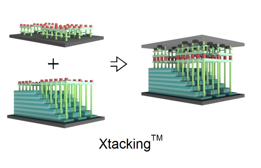
YMTC has identified three benefits of this technology.
The first is to increase the operating speed of the input and output circuits. By using a separate wafer, peripheral circuits such as input/output circuits can be manufactured using CMOS logic processes that can operate at high speeds.
The second is to increase the number of bits per unit area. In other words, if the same number of bits, the area can be reduced. This is because when the memory cell array and peripheral circuits are made on the same wafer, 20 ~ 30% is normally required for the peripheral circuits, but since the peripheral circuits are made on different chips, the memory cell array can be made in an empty space.
The third is to improve development efficiency. Since memory cell arrays and peripheral circuits can be developed and manufactured independently, various variations of products can be manufactured in short TAT by changing the combination of peripheral circuits and memory cell arrays depending on the application.
The strategy is to use this technology to differentiate itself from leading NAND flash memory manufacturers such as Samsung, Kioxia, Micron, and SK-Hynix.
By the way, it is often said that the weak point of Chinese semiconductor companies is that they lack intellectual property. How many patents does YMTC have? We used the Lens, a free patent search database, to find out. Here are the results of a search(As of April 8, 2020) on YMTC and its predecessor XMC.
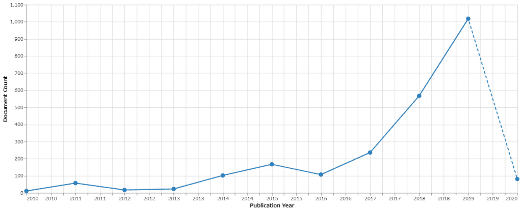
Below is the graph of the number of publications by year. This indicates that the number of patents increased significantly between 2017 and 2019, and that the Company is strengthening its patent portfolio. Most of the published literature seems to be from China. I would also like to see the contents of the portfolio and the contents of individual patents. I’ll try another time about that.
That’s all for this time.