Next-generation transistor structure GAA and pioneer patents
On November 11, 2022, the Ministry of Economy, Trade and Industry (METI) decided that Rapidus Co., Ltd. (hereinafter referred to as “Rapidus”) will be selected for the R&D project to establish a manufacturing infrastructure for next-generation semiconductors (“(2) Development of advanced semiconductor manufacturing technology” in the “Post-5G Information and Communication System Infrastructure Enhancement R&D Project”).
Rapidus is a newly established company with the investment of eight companies, KIOXIA, Sony Group, SoftBank, Denso, Toyota Motor Corporation, NEC, NTT, and MUFG Bank, aiming to launch a foundry business for Japan’s first cutting-edge logic semiconductors. To achieve this, the first thing that is necessary is the establishment of state-of-the-art transistor manufacturing technology.
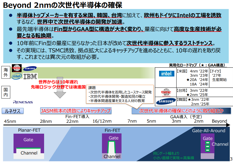
Next-generation transistor structure GAA (Gate-All-Around)
In the cutting-edge semiconductors after 2nm process node that Rapidus is aiming for, it is assumed that the transistor structure will change significantly from a structure called Fin-FET to a structure called GAA (Gate-All-Around). The transistor structure used a planar type MOSFET structure until the 22/28nm generation, but it is expected that a Fin-FET type MOSFET structure will be adopted after 16nm, and a horizontal GAA type MOSFET structure will be adopted after 2nm generation.
Major semiconductor companies and research institutes are developing transistors that can achieve sufficient performance and are easy to manufacture by optimizing the channel shape and material of horizontal GAA.
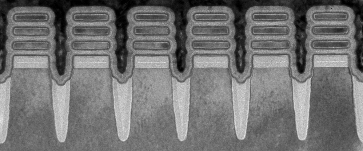
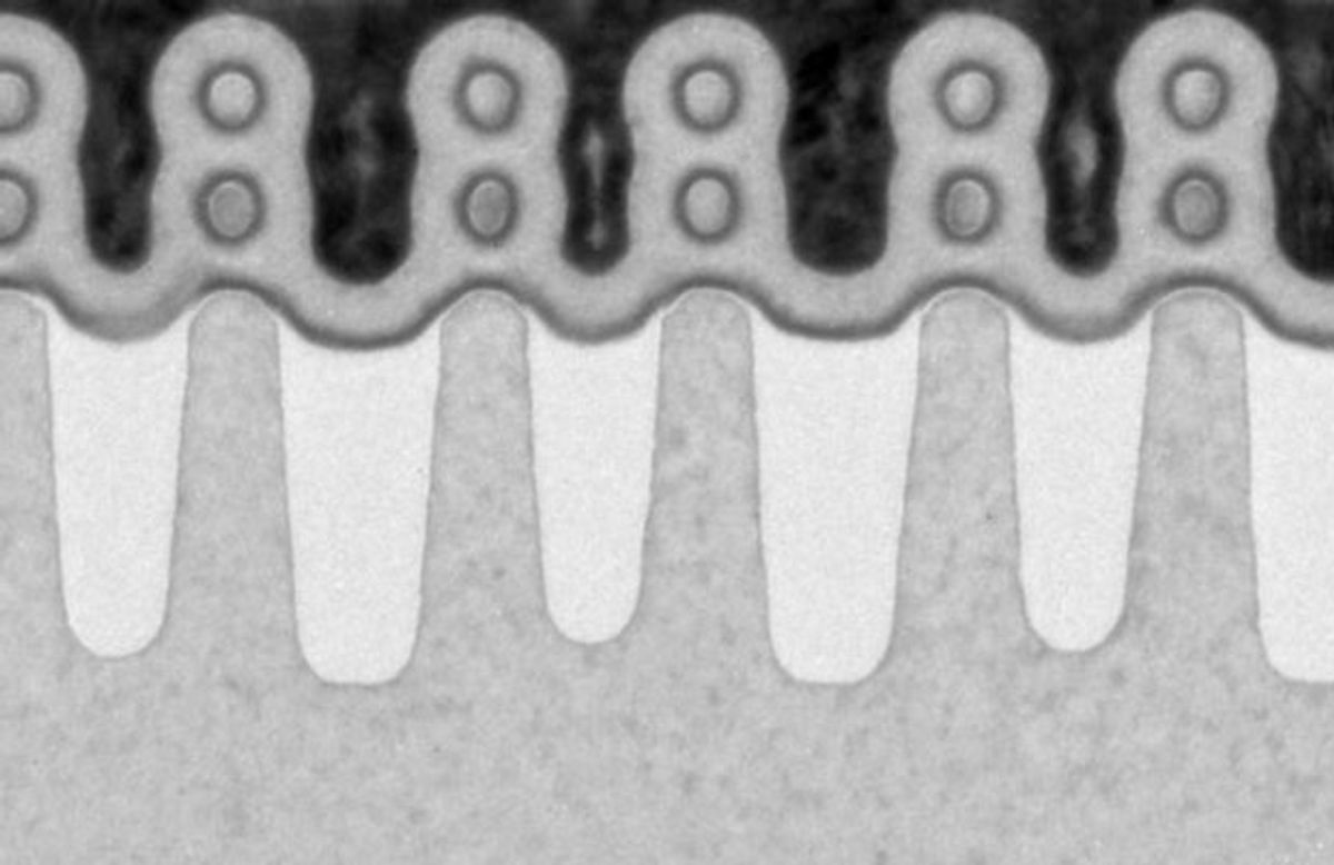
The dominant horizontal GAA structures are nanosheet structures and nanowire structures. The difference is the structure of the silicon channel portion, and the nanosheet type has a flat sheet structure in the channel part, while the nanowire type has a tube structure. The state-of-the-art transistor structure developed by IBM Inc. of the United States, which is considered a partner of Lapidus, is also a nanosheet type GAA. Multiple sheet-shaped channel areas are arranged vertically, and each channel area is surrounded by a gate. In addition, the structure called Multi-Bridge-Channel FET (MBCFET), which Samsung introduced as a 3nm process, is also a nanosheet structure GAA. The future mainstream is considered to be nanosheet structures.
Introduction of Pioneer Patents for Transistor Structure
As already mentioned, the structure of transistors in advanced logic semiconductors begins with the planar type, and is about to move to the GAA type via the Fin-FET type. This time, I would like to introduce some pioneer patents related to transistor structure during this transition.
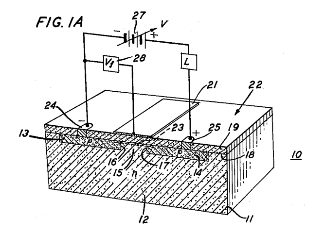
First, the first generation of them is planar MOSFET transistor. The planar type is so called because the channel region is formed on the surface of the semiconductor substrate. The structure was invented in 1959 by D. Kahn and M.M. Atalla of Bell Telephone Labs. However, each initial patent application is filed separately.
The first application was filed by Atala, and on March 8, 1960, which was filed in the United States as Ser. No.13,688 and patented as U.S. Patent No. 3,206,670 on September 14, 1965. Khan, on the other hand, filed in the United States(Ser. No… 32.801) on May 31, 1960, slightly later than Atalla and was patented as U.S. Patent No. 3,102,230 on August 27, 1963.
Although this structure proposed by Khan and Atalla has been partially replaced by the Fin-FET type this time, which will be described later, it is still used in many semiconductor integrated circuits and is one of the most impactful inventions related to semiconductor devices.
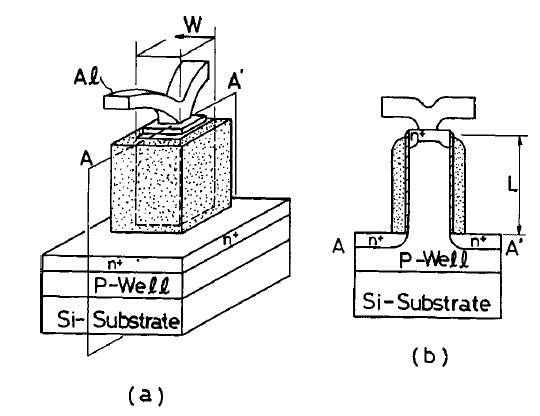
Next is the Fin-FET structure. The DELTA transistor proposed by a research group at the International Conference on Electronic Devices (IEDM) in 1989 is said to be the first Fin-FET structure transistor. Hitachi, Ltd. filed a patent application (Japanese Patent Application S63-292499) with Japan on November 21, 1988, followed by a patent application (H1-045403) on February 28, 1989, based on this application as the basis of the priority claim, and received patent No. 2768719 on April 10, 1998. Later, Fin-FET structures were first mass-produced in 2011 on Intel’s 22nm process.
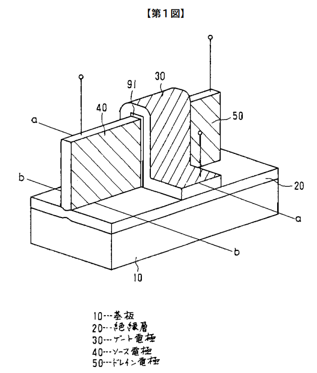
In addition, the prior arts(JP-A-1-8670, JP-A-64-27270) cited in the examination process of the Hitachi’s patent application also disclose a structure in which gate electrodes surround the Fin-like channel region on three sides.


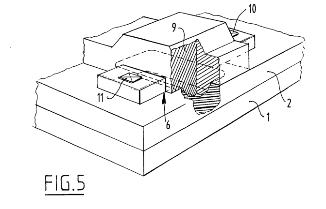
Finally, The GAA structure was proposed by Toshiba research group in 1988 under the name Surrounding Gate Transistor (SGT) and reported in IEEE Transactions on Electron Devices. Inventors include Fujio Masuoka who is well known as the inventor of flash memory. Toshiba filed a patent application (Japanese Patent Application No. S63-223008) on September 6, 1988, and received patent No. 3057661 on April 10, 1998. Toshiba’s invention is the so-called vertical GAA, which forms channels vertically. Although vertical GAA has already been put to practical use as a memory cell for 3D NAND flash memory, it has not yet been put to practical use in the advanced fine semiconductor process that constitutes CMOS logic circuits, and it is considered to be a technology after horizontal GAA.
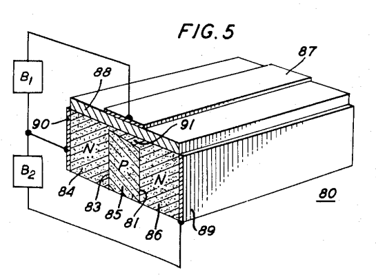
On the other hand, the existence of a horizontal GAA patent application can be confirmed since around 1989. One of the earliest patent applications for horizontal GAA is the Dutch application (NL8902372A) filed by IMEC (Interuniversity Microelectronics Centre) on September 21, 1989. In this invention, an opening is provided in the silicon oxide film (2) directly below the silicon channel film formed by separating from the silicon substrate (1) by a manufacturing method called SIMOX (Separation by Implanted Oxygen), and the opening is used to surround the silicon channel film with a gate electrode. It is quite different from the structure of nanosheets and nanowires that are currently expected to become mainstream. Applications for nanosheet structures and nanowire structures have been confirmed since around 2002.
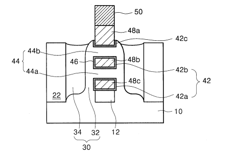
KR100481209B1 Fig. 2.b
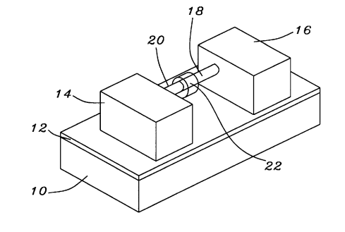
US6583014B1 Fig. 3